Technology Academy Finland (TAF) awards the global one-million-euro Millennium Technology Prize and runs associated events and initiatives.
The Millennium Technology Prize is the preeminent €1 million award focused on technological innovations for a better life. The winning innovations are scientifically rigorous, globally accessible, and uniquely significant in their field.
Voicing public debate on the significance of technology and promoting innovations for a better life
Providing a neutral collaboration forum for business, academia and governmental organizations
Encouraging young people to study and choose a career in technology
One of TAF’s strengths is the tripartite cooperation between industry, governmental organizations and the scientific community and its extensive network in all these sectors. The three sectors are also represented in the TAF Board and in the different committees.
TAF started operating under the name of the Finnish Technology Award Foundation in 2003. In 2005, the name changed to the Millennium Prize Foundation. The name was changed to the Technology Academy Finland in 2008.
TAF’s mission:
Technology Academy Finland (TAF) governs and develops the Millennium Technology Prize, increases public awareness of the Prize and ensures its high academic standard. TAF provides an international meeting ground for corporate life, academia and policymakers, and improves Finland’s position in the global community.
The Board ensures that the foundation’s activities are executed in a proper manner and that the organisation’s funds are invested in safe and appropriate ways. The Board is also responsible for appointing the foundation’s President and CEO and members of the Executive Committee.
Founding organisations
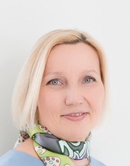
Minna Palmroth
Chair of the board, Professor, University of Helsinki
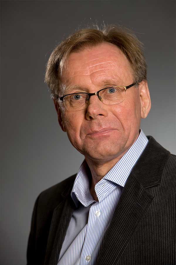
Mikko Hupa
The Swedish Academy of Engineering Sciences in Finland STV
Juho Malmberg
The Finnish Foundation for Technology Promotion TES, Chair of the Board
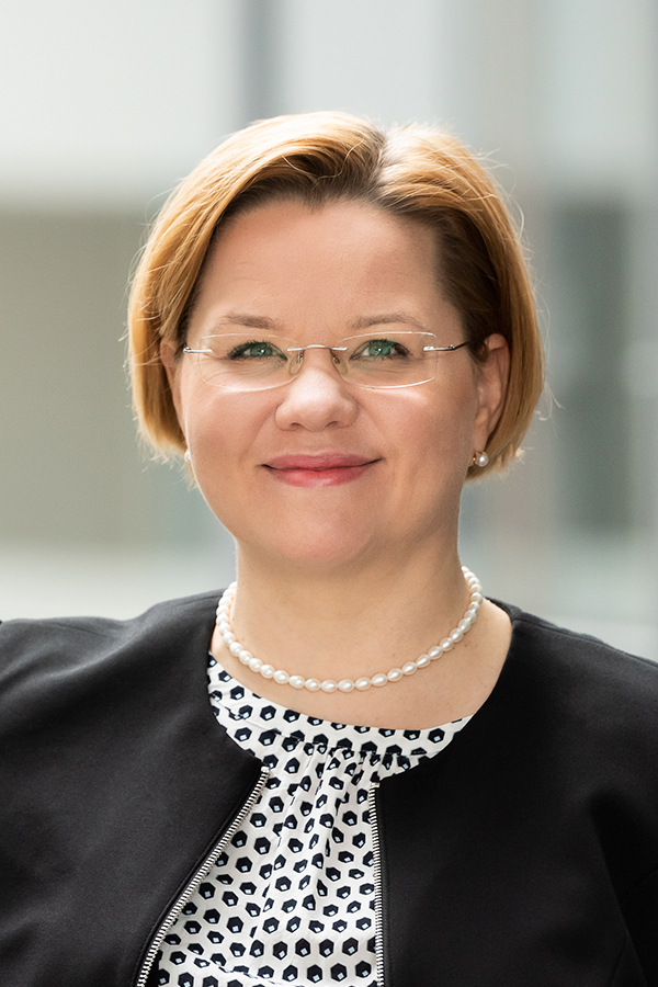
Marjo Matikainen-Kallström
Representative of Academic Engineers and Architects in Finland TEK
Trade and industry
Manja Ahola
Representative of Confederation of Finnish Industries EK
Tapani Kiiski
Representative of the Federation of Finnish Technology Industries
Päivi Leiwo
Member of the Board Federation of Finnish Technology Industries
Marjo Miettinen
Member of the Board Confederation of Finnish Industries EK
Government
Nina Kopola
Director General, Business Finland
Anita Lehikoinen
Permanent Secretary, Ministry of Education and Culture
Jarkko Levasma
Government Chief Information Officer, Director General, Ministry of Finance
Universities
Keijo Hämäläinen
Rector, Tampere University
Sari Lindblom
Rector, University of Helsinki
Mikael Lindfelt
Rector, Åbo Akademi University
Jouko Niinimäki
Rector, University of Oulu
Minna Palmroth
Chair of the board, Professor, University of Helsinki
Mikko Hupa
The Swedish Academy of Engineering Sciences in Finland STV
Päivi Leiwo
Member of the Board Federation of Finnish Technology Industries
Secretary
Markku Ellilä, CEO, Technology Academy Finland
Chair
Timo Leino
LL.M., Chairman of the Board Linnea Capital Oy
Marjo Miettinen
Member of the Board Confederation of Finnish Industries EK
Markku Ellilä
CEO
Marjo Matikainen-Kallström
Representative of Academic Engineers and Architects in Finland TEK
Mission of the Committee is to identify and define the innovation branch in Finland and the most significant phenomena for it. The Committee aims to run a diverse discussion on the issue from different point of views in order that Technology Academy Finland for its part can promote the issue on a most prominent way for Finland.
The Committee acts like a think tank, meetings are being held at least two times a year.
Chair of the committee
Riikka Heikinheimo, Confederation of Finnish Industries EK
Members
Universities
Mika Hannula, University of Turku
Janne Laine, Aalto University
Jukka Mönkkönen, University of Eastern Finland
Anne Portaankorva, University of Helsinki
Jarmo Takala, University of Tampere
Trade and industry
Saara Hassinen, Federation of Finnish Technology Industries
Jaana Hyvärinen, Kone
Harri Junttila, Alma Talent
Hannu Kauppinen, Nokia
Lars Peter Lindfors, Neste
Johanna Sipola, International Chamber of Commerce
Petri Takala, Academic Engineers and Architects TEK
Hannu Talvitie, Vaisala
Markku Teräsvasara, Metso
Pekka Tiitinen, ABB
Academies
Markku Ellilä, Technology Academy Finland
Mika Hannula, Finnish Academy of Technical Sciences
Mikko Hupa, The Swedish Academy of Engineering Sciences in Finland
Risto Nieminen, Finnish Academy of Science and Letters
Public sector and decision makers
Mikko Dufva, Sitra
Erja Heikkinen, Ministry of Education and Culture
Riitta Maijala, Academy of Finland
Antti Pelkonen, Prime Minister’s Office
Päivi Sillanaukee, Ministry of Social Affairs and Health
Heikki Uusi-Honko, Business Finland
Secretary: Markku Ellilä, Technology Academy Finland
The Communication Committee’s mission is to highlight the importance of research, knowledge and innovation for the well-being and future development of society, and to promote Finland as a high-tech country. The members of the Committee represent Millennium Technology Prize partner universities and companies, Ministry of Foreign Affairs of Finland, Sitra (the Finnish Innovation Fund), Business Finland, TEK (Academic Engineers and Architects in Finland), Healthtech Finland and the Research Council of Finland.
Chair of the Committee:
Saara Hassinen, CEO, Healthtech Finland, Federation of Finnish Technology Industries
Members:
Thurid Eriksson, Director of Communications, Åbo Akademi University
Katrina Jurva, Head of Content and Media, Aalto University
Tuomas Koivula, Managing Editor, University of Turku
Liisa Kuvaja, Brand and Communications Director, LUT University
Risto Löf, Head of Communications, University of Eastern Finland
Johanna Pellinen, Communications Manager, University of Helsinki
Hanna-Mari Soini, Director of Marketing and Communications, University of Vaasa
Anna-Kaisa Säkkinen, Director of Communications, University of Jyväskylä
Anni Ylinen, Communications Specialist, Tampere University
Ville Wittenberg, Science Communications Specialist, University of Oulu
Kaisa Antikainen, Communications Manager, Nokia
Johanna Fräki, Head of Open Innovation and Innovation Marketing, Neste
Jenni Hovi-Seppä, Marketing Manager, Alma Talent
Tommi Manninen, SVP, communications and public affairs, Enersense
Helena Marjaranta, VP, Communications & Brand, Metso
Aleksi Moisio, Communications Lead, OP Financial Group
Mira Nupponen, Global Communications Manager & Business Partner, Kone
Satu Perälampi, Head of Country Communications, ABB
Tarja Österberg, Communications Manager, Vaisala
Pinja Hentunen, Communications Specialist, Research Council of Finland
Tomi Korhonen, Executive Director, Communications, Business Finland
Kirsi Vanamo-Santacruz, Deputy Director General, Department for Communications, Ministry for Foreign Affairs
Markku Ellilä, CEO, Technology Academy Finland
Laura Manas, Communications Manager, Technology Academy Finland
Minna Zaknoun, Communications assistant, Technology Academy Finland
More information: Laura Manas Communications Manager, Technology Academy Finland laura.manas@millenniumprize.org +358 500 989 286
Technology Academy Finland is a participant of the UN Global Compact initiative that supports the United Nations’ universal principles and Sustainable Development Goals. It has more than 17 000 member organizations around the world.